
| Introduction | |||||
|
In this assignment, you will be developing a structural model for the DCT chip in VHDL. You are provided with a primitive Register Transfer (RT) component library. The VHDL model and the delay for each component is given. You will be instantiating components from the library and developing the chip model. You will learn the hierarchial design methodology in structural VHDL by developing and simulating models for the DCT chip. This assignment has 2 parts. The first part is due 1 week from now (on June 3rd) and the second part is due 4 weeks from now (on June 12th, the last day the lab is open).
|
|||||
| Structural Model | |||||
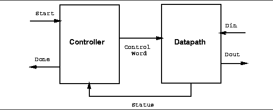
As shown in Figure 1, the structural view of the sequential design is decomposed into two parts, namely controller and datapath. The controller generates a set of control signals grouped as control word which controls the datapath. The datapath send a status word to the controller. The status signals helps in determining the next state and control signals generated. In the DCT example, the status word consists of the nine bits of the count register. |
|||||
| Datapath Routing | |||||
|
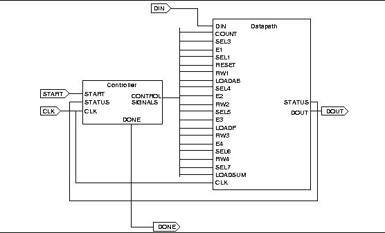
The top-level view of the DCT chip is shown in Figure 2. Note that the entire design has been partitioned into a controller and a datapath. The controller is in-turn modelled as shown in Figure 3. The controller is a finite-state machine with a State Register (described in the str.vhd file), Next State and Output Logic (described in the logic.vhd file).
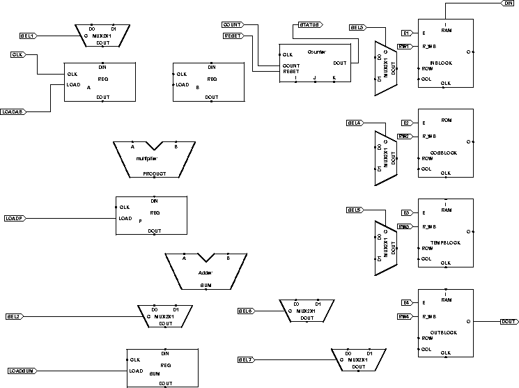
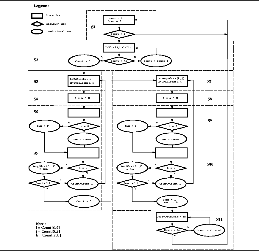
In the first part of this lab assignment, you are required to figure out the datapath interconnections given the controller model and the unconnected datapath shown in Figure 4 executing the behavior given in Figure 5. You are required to finish an incomplete datapath schematic drawn in Synopsys Schematic Editor. For this part you just need to complete the schematic. All other parts of the DCT chip are provided and are correct. Finish the wiring and generate the VHDL code for the datapath. The code for the datapath can generated easily using the Synopsys tools if the datapath has been wired correctly (as done in the first tutorial assignment). Compile the code for the datapath, the controller with the test bench together and observe the simulation results.
|
|||||
| Performance Optimizations | |||||
|
In Lab assignment 2, you used Chaining, Multicycling and Loop Unrolling to improve the performance. In Lab assignment 3, you used Pipelining to further improve the performance of the design. In this part, you will design and simulate a structural model for the controller and the datapath for the best optimized DCT design that you developed in assignment 3. You may need to change the datapath schematic that you completed for part 1 of this assigment. The controller model will then need to be changed inorder to provide the correct control signals for the optimized design.
|
|||||
| Assignment for Lab 4 | |||||
|
|||||
| Assignment for Lab 5 | |||||
|
|||||
| Report for Lab 4 | |||||
|
|||||
| Report for Lab 5 | |||||
|
|||||
| Source Listing for Component Library | |||||
A.1 comp.vhdA.2 adder.vhdA.3 multiplier.vhdA.4 mux2x1.vhdA.5 reg.vhdA.6 counter.vhdA.7 rom.vhdA.8 ram.vhdA.9 controller.vhdA.10 str.vhdThis file has the source code for the State Register used inside the controller for storing the current state of the controller.A.11 logic.vhdThis file has the VHDL source code for the Next State and Output Logic used inside the controller for determining the next state and output of the controller.A.12 clock_gr.vhd |
|||||