
| Objective | |||
|
In this lab, you are provided with the VHDL behavioral model of the DCT chip you're going to model for the rest of this quarter.
A simple test bench with one test pattern is also provided. You are required to debug the model and understand the behavioral
modeling. You are also required to write another test pattern. This test pattern will be used in the other two labs.
|
|||
| Problem Specification | |||
|
Discrete Cosine Transform (DCT) is often a critical part in both still and motion picture compression. The definition of DCT for a
N × N image is as follows:
where:
u, v = discrete frequency variables ( As shown in the code below, DCT is basically two consecutive matrix multiplications. In our design we will assume that N = 8. In this case, C will be a 8 × 8 matrix defined as
Furthermore, let COS1 be integer matrix defined as COS1 = round(factor * C) and COS2 be its transpose: COS2 = COS1T Let f be the 8 × 8 input block of image, and F be the output matrix, then F = COS1 × f × COS2
int   COS1[8][8], COS2[8][8];


void  MatrixMult (int a[][8], int b[][8[], int c[][8]) {


    register int   i, j, k;


    for (i=0; i<8; i++)

       for (j=0; j<8; j++) {

          c[i][j] = 0;

          for (k=0; k<8; k++)

             c[i][j] += a[i][k] * b[k][j];

       }

}


void  DCT (int f[][8], int F[][8]) {


   int  Temp[8][8];


   MatrixMult(f, COS2, Temp);

   MatrixMult(COS1, Temp, F);

}
|
|||
| Interface Specification | |||
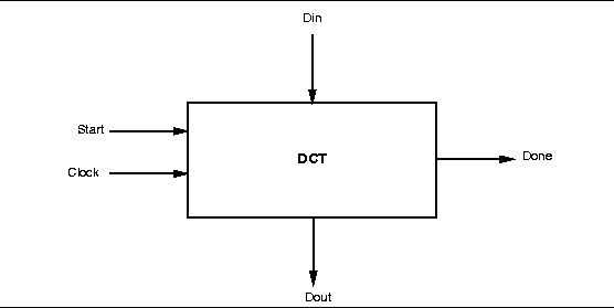
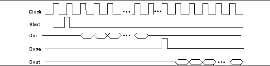
As shown in Figure 1, the interface of the DCT chip consists of a pair of hand-shake ports ``Start'', which indicate the start of the computation, and ``Done'', which indicate the end of the computation. The chip also has a input data port and a output data port.
Figure 2 shows the timing protocol. The image block is inputed to the Din port on a cycle by cycle basis after the ``Start'' signal becomes equal to 1. Note that it takes 64 clock cycles for the 8 by 8 matrix. Similarly, the output data appears on the Dout port on a cycle by cycle basis after the ``Done'' signal is equal to 1. Note that it also takes 64 clock cycles for the 8 by 8 matrix to be outputed. |
|||
| Testing Strategy | |||
|
Generally speaking, our testing strategy is to include some
typical scenario and an exhaustive test of boundary conditions.
As for this particular DCT application, the computation is characterized by nested loops and is rather regular, a careful selection of one input matrix can cover most of problems concerned. VHDL assert statement is used to specify the expected output, which is obtained by the corresponding output of a C program. The test matrix chosen here is an block which looks like a sandwich. The cheese part is ``black'' with the gray level equal to 0, while the rest is ``white'' with the gray level equal to 255. Note that these are minimum and maximum gray levels the image can have. 255 255 255 255 255 255 255 255 255 255 255 255 255 255 255 255 255 255 255 255 255 255 255 255 0 0 0 0 0 0 0 0 0 0 0 0 0 0 0 0 255 255 255 255 255 255 255 255 255 255 255 255 255 255 255 255 255 255 255 255 255 255 255 255 |
|||
| VHDL Behavioral Model | |||
|
The VHDL model developed here consists of a DCT entity which models the DCT chip and a test bench. The DCT entity has a clock port, two handshake ports Start and Done, input data port Din and output data port Dout. Since the bitwidth of the data will be determined later, we models Din and Dout as integer types. The testbench includes the DCT chip and a clock generator as its components. It generates the handshake signals, then feeds the test data into the chip, and finally verifies the output data. |
|||
| Getting Started | |||
|
Your Environment
Set up the environment for Synopsys VHDL tools by adding ``module load synopsys/2001.09'' in the .cshrc file under your home directory if you have not done so yet. Create a directory called WORK in your home directory, and create a file called .synopsys_vss.setup in your home directory containing the following five lines (make sure the last line is terminated by a newline):
    WORK > DEFAULT

    DEFAULT : ~/WORK

    TIMEBASE = ns

    CS_COMPILED = FALSE

    CS_COMPILED_WARN = FALSE
Get the Source Code
Get the VHDL models by visiting the link below: http://www.cecs.uci.edu/~gajski/ics155b/lab1/files/ Analyze and Simulate Compile the models as follows (note that the % denotes the UNIX command prompt):% vhdlan -nc -ccpath /opt/gcc-2.95.2/bin/gcc clock.vhd dct.vhd tb.vhd NOTE: The files have to be compiled in the order specified!!, i.e. if an entry declared in a file a.vhd is instantiated in file b.vhd then b.vhd should be compiled AFTER a.vhd. If there is no compilation error, you can generate makefile and simulate the circuit as follows: % simdepends TB__TEST > makefile % vhdldbx TB__TEST &A simulation window will appear on the screen. This consists of 3 main parts. The top region shows your VHDL code. The middle region is for messages. The bottom line of the window is for command entry. Type in the following command for simulation: # trace *'sigA new window will be launched with every top level signal name in it. This window will display the waveforms generated as a result of the simulation. # run 'number'4000 is recommended for the 'number'. Check the result in the wave window and see if there is any error message in the message region. If there is an error in the DCT component, it will generate incorrect results. Thus, the output will not match the expected output, listed in the test bench. The message region will list these as mis-match errors. If mismatches occur, modify the VHDL file and recompile it in another window. After recompilation, restart the simulation by selecting Execute->Restart, then clicking OK if the TB__TEST is selected already or after selecting this design. Then type the command ``run number'' in the simulation window as before. DebugYou should observe that wrong results are generated after the Done signal goes high and the debugger reports them as errors. Try to debug the model and get the correct result. |
|||
| Your Turn-in Report | |||
|
|||
| Source Listing | |||
| VHDL model for a dct chip - dct.vhd Test Bench - tb.vhd Clock Generator - clock.vhd | |||